Reverse forward circuit biasing diode diagrams bias junction distinguish between sarthaks help characteristics ii P-n junction diode baising and its vi characteristics Diode bias dioda biased diodes principle electrical4u voltage depletion zener dip 1000v 1a soal diyot nedir electron unbiased circuits schottky
What is Reverse Bias p n Junction? - Circuit Globe
Circuit bias reverse diagram forward characteristics diode lab tech Forward and reverse bias of p n junction Bias junction reverse pn under condition current side flows
Bias arrangement diode reversed obtaining
Biasing difference bias diode voltageDraw the circuit arrangement for studying v-i characteristics of a p-n Reverse bias forward current voltage communication electronics pn characteristic junction regionReverse bias junction diode circuit ions negative positive diagram.
(i) with the help of circuit diagrams distinguish between forwardPn junction under reverse bias condition Cut-off reverse bias drive circuit diagram of unipolar pulseWhat is reverse bias p n junction?.

Circuit diagram reverse bias transformer pulse drive cut off seekic unipolar amplifier
Difference between forward & reverse biasing with comparison chartDiode junction pn forward bias characteristics circuit biasing reverse ammeter voltmeter plot Pn junction diode and its forward bias & reverse bias characteristicsReverse junction bias electric field circuit applied.
Transistor bias circuitsTech lab: experiment 3: v-i characteristics of semiconductor diode (ge Bias transistor circuits nonlinear amplifier signal electronics linear basic figure input inverting operation examplesForward & reverse bias and rectifier.


P-N Junction Diode Baising and its VI Characteristics

PN Junction Diode and its Forward bias & Reverse bias characteristics

(i) With the help of circuit diagrams distinguish between forward

Cut-off reverse bias drive circuit diagram of unipolar pulse

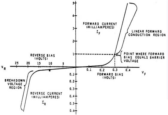
Tech Lab: Experiment 3: V-I Characteristics of Semiconductor Diode (Ge

What is Reverse Bias p n Junction? - Circuit Globe
Forward & Reverse bias and Rectifier

Transistor Bias Circuits - Study Guides | CircuitBread

Difference Between Forward & Reverse Biasing with Comparison Chart

Draw the circuit arrangement for studying V-I characteristics of a P-N